iPcb会社-信頼できるPCBメーカー! お問い合わせ

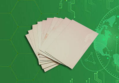
f4bmx- 1/2は輸入テフロン樹脂とテフロン樹脂の複合ガラスシートを使用し、科学的なレシピと厳格なプロセスフローに基づいて作られています。f4bシリーズに比べて誘電率範囲が広いこと、誘電損失角接線が低いこと、抵抗が大きいこと、性能が安定していることなどを特長とする。f4bmと比較して,輸入ガラス机器を用いて織布することで,ラミネート板の各性能の一貫性を確保することができる。
技術仕様:
Appearance | Meet the specification requirements for the laminate of microwave PCB by National and Military Standards. | ||||||||||||||||||
Types | F4BMX217 | F4BMX220 | F4BMX245 | F4BMX255 | F4BMX265 | F4BMX275 | |||||||||||||
Dielectric Constant | 2.17 | 2.20 | 2.45 | 2.55 | 2.65 | 2.75 | |||||||||||||
Types | F4BMX285 | F4BMX294 | F4BMX300 | ||||||||||||||||
Dielectric Constant | 2.85 | 2.94 | 3.0 | ||||||||||||||||
Dimension(mm) | 300×250 380×350 440×550 500×500 460×610 600×500 840×840 840×1200 1500×1000 1800×1000 | ||||||||||||||||||
For special dimension,customized laminates is available. | |||||||||||||||||||
Thickness and Tolerance(mm) | Laminate thickness | 0.25 | 0.5 | 0.8 | 1.0 | ||||||||||||||
Tolerance | ±0.025 | ±0.05 | ±0.05 | ±0.05 | |||||||||||||||
Laminate thickness | 1.5 | 2.0 | 3.0 | 4.0 | 5.0 | ||||||||||||||
Tolerance | ±0.05 | ±0.075 | ±0.09 | ±0.10 | ±0.10 | ||||||||||||||
Laminate thickness | 6.0 | 8.0 | 10.0 | 12.0 | (Thickness≥5.0mm,dimension≤600x500 ) | ||||||||||||||
Tolerance | ±0.12 | ±0.15 | ±0.18 | ±0.2 | |||||||||||||||
The laminate thickness includes the copper thickness. For special dimension,customized laminates is available. | |||||||||||||||||||
Mechanical Strength | Warp | Thickness(mm) | Maximum Warp | ||||||||||||||||
Original board | Single side | Double side | |||||||||||||||||
0.25~0.5 | 0.030 | 0.050 | 0.025 | ||||||||||||||||
0.8~1.0 | 0.025 | 0.030 | 0.020 | ||||||||||||||||
1.5~2.0 | 0.020 | 0.025 | 0.015 | ||||||||||||||||
3.0~5.0 | 0.015 | 0.020 | 0.010 | ||||||||||||||||
Cutting/punching Strength | Thickness1mm,no burrs after cutting,minimum space between two punching holes is 0.55mm,no delamination. | ||||||||||||||||||
Thickness1mm,no burrs after cutting,minimum space between two punching holes is 1.10mm,no delamination. | |||||||||||||||||||
Peel strength(1oz copper) | Normal state:≥18N/cm;No bubble、delamination、peel strength≥15N/cm(in the constant humidity and temperature、and keep in the melting solder of 260℃±2℃ for 20 seconds). | ||||||||||||||||||
Chemical Property | According to the properties of laminate,the chemical etching method for PCB can be used. The dielectric properties of laminate are not changed. The plating through hole can be done,but the sodium treatment or the plasma treatment must be used. The Hot Air Level temperature can not be higher than 253℃,and can not be repeated. | ||||||||||||||||||
Electrical Property | Name | Test condition | Unit | Value | |||||||||||||||
Density | Normal state | g/ cm3 | 2.1~2.35 | ||||||||||||||||
Moisture Absorption | Dip in the distilled water of 20±2℃ for24 hours | % | ≤0.08 | ||||||||||||||||
Operating Temperature | High-low temperature chamber | ℃ | -50℃~+260℃ | ||||||||||||||||
Thermal Conductivity | W/m/k | 0.3~0.5 | |||||||||||||||||
CTE (typical) | 0~100℃ (εr :2.1~2.3) | ppm/℃ | 24(x) | ||||||||||||||||
34(y) | |||||||||||||||||||
235(z) | |||||||||||||||||||
CTE (typical) | 0~100℃ (εr :2.3~2.9) | ppm/℃ | 16(x) | ||||||||||||||||
20(y) | |||||||||||||||||||
168(z) | |||||||||||||||||||
CTE (typical) | 0~100℃ (εr :2.9~3.38) | ppm/℃ | 12(x) | ||||||||||||||||
15(y) | |||||||||||||||||||
92(z) | |||||||||||||||||||
Shrinkage Factor | 2 hours in boiling water | % | 0.0002 | ||||||||||||||||
Surface Resistivity | 500V DC | Normal state | M·Ω | ≥2×10⁵ | |||||||||||||||
Constant humidity and temperature | ≥8×10⁴ | ||||||||||||||||||
Volume Resistivity | Normal state | MΩ.cm | ≥8×10⁶ | ||||||||||||||||
Constant humidity and temperature | ≥2×10⁵ | ||||||||||||||||||
Surface dielectric strength | Normal state | d=1mm(Kv/mm) | ≥1.2 | ||||||||||||||||
Constant humidity and temperature | ≥1.1 | ||||||||||||||||||
Dielectric Constant | 10GHZ | εr | 2.17,2.20,2.45,2.55,2.65,2.75,2.85,2.95,3.0。 (±2%) | ||||||||||||||||
Dissipation Factor | 10GHZ | tgδ | 2.172.2 | ≤1×10⁻³ | |||||||||||||||
2.453.0 | ≤1.4×10⁻³ | ||||||||||||||||||

ホームページをご覧くださいhttps://www.ipcb.com
ipcb.comの製品:
無線周波数/マイクロ波/混合高周波、fr4ダブル/多層、1~3+ n +3 hdi、任意の層hdi、剛柔、ブラインド埋め、ブラインド溝、バックドリル、ic、銅板など。
*何か問題があれば、www.ipcb.comを通じて私達と連絡してください、私達はできるだけ早くあなたに返信します。
*問い合わせは直接sales@ipcb.comまでお送りします
マイクロ波無線周波数pcbが必要な場合は、マイクロ波回路をクリックしてください。
